CRU: is a high-tech unit, which provides the crucial interface between detector front-end electronics and DAQ by performing data aggregation and distribution of timing, trigger and control information. Each unit provides 48 bidirectional high-speed links running at 10 Gbits/s. It consists of a sophisticated Intel Arria 10 FPGA with about 1900 components.
Technical benefits
- Development in electronics, FPGA applications and high-speed data acquisition.
- Knowhow on the integration of a large number of high-speed links on the state-of-the art 20 nm FPGA with a large number of logic resources. potential applications in various programs in the country, especially for data acquisition in high radiation zones.
Complexity of the Common Readout project arises because of the three aspects of this project. First is the intricacy, which arises due to the (A) design requirements, second due to the (B) hardware requirement of this board that guides its fabrication challenges and third arises due to the stringent (C) firmware design specifications. These three challenge areas are explained below.
Design requirements
- Huge data to be handled (3.3 TB/sec) as already mentioned.
- Total 48 readout link connections per CRU hardware is the highest count of links integrated in a data acquisition board as compared to the earlier used boards. Actual usage however depends on the specific detector e.g.: TPC will utilize 20 such readout links which corresponds to maximum aggregate throughput of 20\(\times\)4.48 Gb/s = 89.6 Gb/s.
- CRU also has to process the data on the fly in FPGA during the transmission before it is being sent to the O2 system via PCIe. The data volume will be reduced by processing the data on the fly with data taking and not by rejecting complete events. The most demanding CRU implementation will be for the TPC due to the high data rate and signal processing (base-line correction, zero-suppression and cluster finding) and then the reduced data is sent further. Data reduction in the online systems results peak data rate to storage of 80 GB/s from raw detector data.
- As CRU is an interface for the different systems in ALICE, it will provide the LHC clock for the Front-End over the GBT downlink. The recovered LHC clock output from the GBTx ASIC must have a constant and deterministic phase relation to the original LHC clock between each GBT links, CRU units, power-on cycles and firmware updates. The maximum acceptable LHC jitter is 300 ps (RMS) and the clock skew should not exceed 1 nano-sec (peak-to-peak) as per requirement of TPC.
Hardware Complexity
- The CRU hardware part is one of the major aspects of this project. The PCIe40 board used as CRU is custom designed for the requirements of the high energy physics applications. It has a large number of transceivers on it (up to 48 optical inputs/outputs, serial signal up to 10 Gb/s), with high density PCIe Gen3 x16 to transfer data to PC.
- To summarize the complexity of this hardware, (a) it is a HDI (High Density Interconnect) PCB with more than 1750 components, (b) it is a 14 layer board with blind, buried and the stacked vias, and laser drills are required for its fabrication. Power requirements are supported by the mezzanine cards, which will be modified in further versions.
- Material requirements for the CRU PCB are also strict. It is a high Tg (Glass Transition Temperature) PCB, Tg is the temperature at which materials begin to expand at an uncontrolled rate. Boards operating beyond Tg are subject to failure. So if the temperature exceeds designated Tg value, the board will change from glassy state to rubbery state and then the function of PCB will be affected. (Tg = 140 C in our case)
- Low dielectric constant (also called as relative permittivity) material for high speed and low loss is required. The dielectric constant Dk is closely related to the impedance of the circuits that will be fabricated on that material. Changes in a PCB material’s Dk , whether as a function of frequency, temperature, or other reasons, can adversely affect the performance of broadband high-frequency high-speed digital as well as analog circuits because it will change the impedances of transmission lines in unexpected ways. In particular, these unwanted changes in Dk and impedance result in distortion to the higher-order harmonics making up a high-speed digital signal, with loss of digital signal integrity. (ISOLA 408 HR, TUC 872 LK are the qualified ones, Er \(\lt\) 3.7 at 5 GHz, Df \(\lt\) 0.012 at 5 GHz)
- Track width requirement is 3 mil (1 mil = 0.001 inch). A 20% change in trace width can cause as much as a 10% change in impedance. As width increases, characteristic impedance decreases. Control of trace width is both a function of process control by the board fabricator and to some degree the type of copper used on the base material. To minimize crosstalk, the distance between two traces should be approximately 2 to 3 times the width of the trace. The minimum via size on the board is 2 mil only and also there are micro-vias, there are via below the pads also that increases the complexity at the production of PCB and even at the component assembly stage.
- This PCB with all these complexities should only be 1.57 mm +/- 10% thick. If they are made thicker then they cannot be inserted in the PCIe slot of the servers.
- The Arria10 FPGA used on this board as decided by the ALICE collaboration is one of the latest available with 20 nm technology from Altera, which itself is a major challenges in terms of performance. It is highly dense with large number of logic resources which is required for experiments/TPC, so when all the links will be tested all together the junction temperature could rise, this could change the trigger latency (it has to be tested first before any claim). Since this FPGA is new in market it is not tested yet in such high usage applications. (There could be even more drawbacks).
- CRU as mentioned earlier is at the core of the data acquisition system through which the trigger, timing, control and data pass, hence these boards has to be highly reliable as its failure during the run time of an experiment will lose some of the precious beam time before getting replaced, an extremely unwanted situation. Hence the components on the board should be highly reliable (role of procurement comes here).
- Few other measures to ensure the reliability of this board are, the firm producing and assembling the PCB must be ISO 9001:2008 certified in the field of production and support of electronic modules. PCB production must be compliant to IPC A600 and test certificate of compliance to this standard must be provided. The Electronic manufacturing service (EMS) must be performed according to CIS IPC A610 class 2 or class 3 standard. Rework of the component assembly if any must comply with IPC A 7711 standard. (IPC, the Association Connecting Electronics Industries, is a trade association whose aim is to standardize the assembly and production requirements of electronic equipment and assemblies. It was founded in 1957 as the Institute for Printed Circuits). (Electronics manufacturing services (EMS) is a term used for companies that test, manufacture, distribute, and provide return/repair services for electronic components and assemblies for original equipment manufacturers (OEMs).)
- For the production of such high-end boards no standard market is available. There are a few customized components that are present on this board, just to mention optical ribbon cable of different lengths will be required with optical fibre connector at one end and the Prizm connector (to turn the light) at the other end.
- Since several components are of latest category and a few are even customized hence procurement delays are expected (e.g.: FPGA has very high lead time, few crucial components could be out of stock).
Firmware complexity
Level of complexity in firmware could be divided in two parts, low level interface and the user logic firmware inside FPGA. A programming interface (API) that is the most detailed, allowing the programmer to manipulate within hardware at a very granular level. So these are at the CRU board level, the PCIe Gen3, 16 lane interface on the board, input transceiver links, GBT interface, the other i2c interfaces that could be programmed etc, and the other part is the user logic or the firmware to be implemented in FPGA. The CRU firmware itself is an assembly and hierarchy of many different firmwares like GBT-FPGA (firmware that receives the data inside FPGA from GBT chipset), Trigger Timing and Control over Passive optical networks (TTC-PON) and the PCIe interface firmware logic. The firmware of CRU is quite a complex hierarchical structure, integrating in it the entire flow of communication along with the critical timing requirements for different modules. Whole integrated firmware should work in a synchronous way, if the timing requirements are not met then it will propagate till the top level and in a multiplied fashion. (for e.g.: if the VHDL state machine for reading and writing is not designed in a proper fashion as recommended by the Altera then the clock delay could propagate till the top level in the slow control firmware and will misinterpret the instructions). Its development is quite a challenging task and requires long term expertise.
First PCB Delivered to VECC

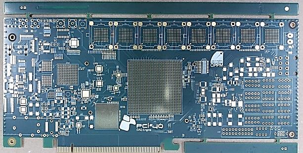
Design Layout of PCB
PCIe40 BOARD IMAGES
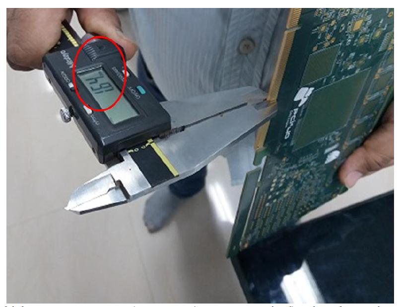
The arrangement for measurement of PCB thickness as this is a crucial parameter for the PCBs to pass the test.
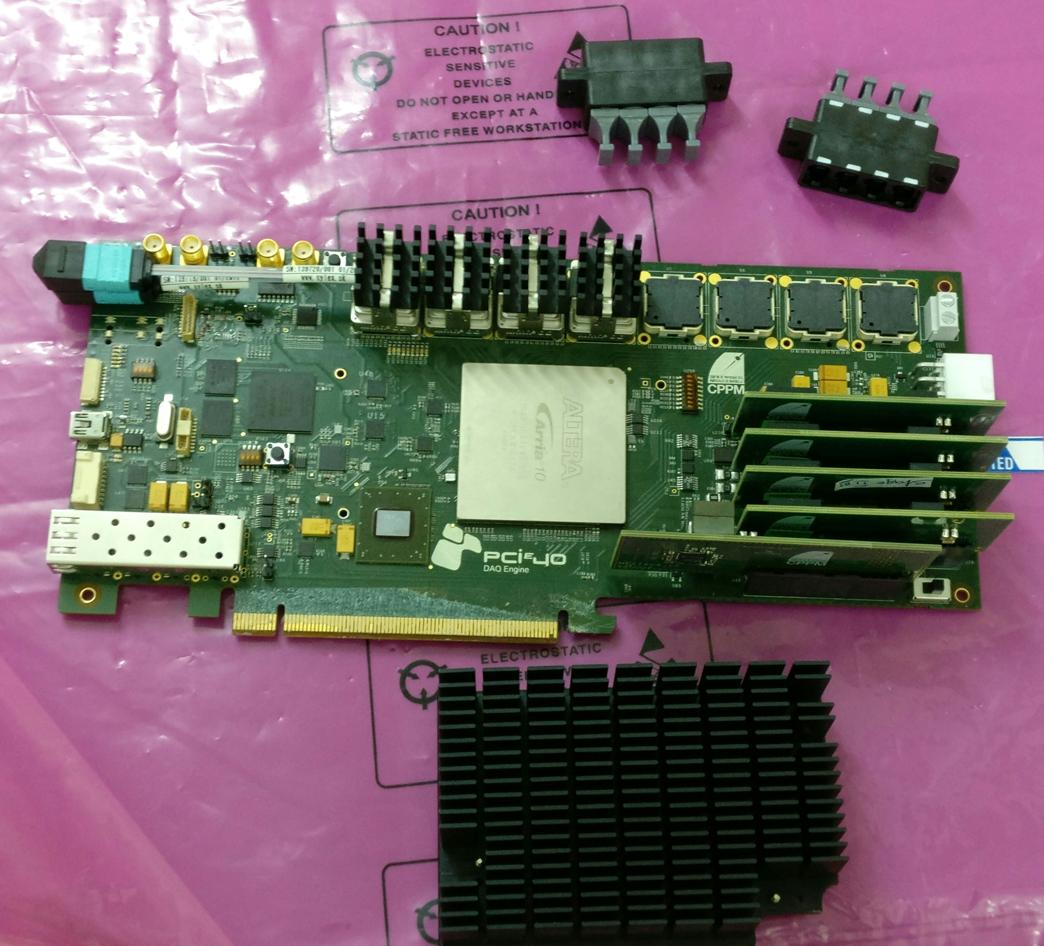
First CRU Board arrived at VECC for testing.

Arria10 development kit

AMC40 testing setup
Deliverables from India
- Two fully assembled prototype-I boards with results of initial tests done at VECC.
- Four bare PCBs
- Two more pre-series prototype boards as per design modifications done with prototype-I boards
- Delivery of 370 CRU boards fully tested. (360 for TPC and 10 for MFT).
- Participation in firmware and software development for CRU as per the requirement of ALICE-CRU team.
Publications
- Reconfigurable very high throughput low latency VLSI (FPGA) design architecture of CRC 32,
INTEGRATION, the VLSI journal 56 (2017) 1-14
https://isiarticles.com/bundles/Article/pre/pdf/144117.pdf - Common Readout Unit (CRU) - A new readout architecture for the ALICE experiment, 2016 JINST
11
C03021
https://iopscience.iop.org/article/10.1088/1748-0221/11/03/C03021 - GBT link testing and performance measurement on PCIe40 and AMC40 custom design FPGA boards,
JINST 11
(2016) 03, C03039
https://doi.org/10.1088/1748-0221/11/03/C03039